

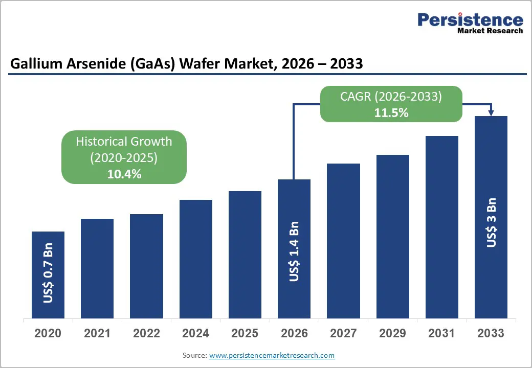
The global Gallium Arsenide (GaAs) wafer market is entering a strong expansion phase, supported by accelerating demand for high-frequency semiconductor devices across telecommunications, defense, aerospace, automotive radar, and satellite communication systems. The market is expected to be valued at approximately US$ 1.4 billion in 2026 and is projected to reach US$ 3.0 billion by 2033, expanding at a CAGR of 11.5% during 2026–2033.
This growth reflects a structural transformation in global connectivity ecosystems, driven by 5G expansion, early 6G research, and rapid adoption of connected devices. GaAs wafers, known for their superior electron mobility and direct bandgap properties, are increasingly preferred over traditional silicon in high-frequency RF applications where signal integrity, power efficiency, and thermal stability are critical.
Market Overview and Growth Drivers
Gallium arsenide wafers are essential substrates used in the fabrication of radio frequency (RF) components, optoelectronic devices, and microwave circuits. Their ability to support high electron mobility enables efficient power amplification and high-speed signal transmission, making them indispensable for modern wireless infrastructure.
The market’s growth is strongly tied to:
- Expansion of 5G and advanced wireless infrastructure
- Rising deployment of satellite broadband constellations
- Increasing adoption of advanced driver-assistance systems (ADAS)
- Military and aerospace modernization programs
- Growing demand for high-frequency RF front-end modules
Global digital transformation and explosive growth in data consumption are further intensifying demand for high-performance semiconductor materials like GaAs.
Key Industry Highlights
- Leading Region (2026): Asia Pacific with ~41% market share
- Fastest Growing Region: Asia Pacific (2026–2033)
- Leading Wafer Type: Liquid Encapsulated Czochralski (LEC) GaAs (~38% revenue share)
- Fastest Growing Wafer Type: Molecular Beam Epitaxy (MBE)
- Top Application Segment: Telecommunications & 5G infrastructure (~41% share)
- Fastest Growing End-Use: Automotive electronics and radar systems
Expansion of 5G and Advanced Wireless Infrastructure
The rollout of 5G networks is one of the most powerful drivers of GaAs wafer demand. Telecom operators are rapidly deploying small cells, massive MIMO systems, and millimeter-wave base stations that require highly efficient RF components.
According to 2025 industry data, over 3,378 5G devices have been announced globally, with nearly 88% commercially available, reflecting rapid ecosystem maturity and adoption growth.
GaAs wafers play a critical role in:
- RF power amplifiers
- Low-noise amplifiers (LNA)
- Microwave and millimeter-wave circuits
- Front-end modules in smartphones and base stations
Their superior frequency performance compared to silicon makes them essential for next-generation wireless communication systems, especially as networks transition toward ultra-low latency and high-bandwidth applications such as IoT, autonomous systems, and industrial automation.
Defense, Aerospace, and Satellite Communication Modernization
Government defense spending and space communication programs are significantly increasing demand for GaAs-based components. The U.S. Department of Defense (DoD) continues to prioritize R&D investments in advanced radar, secure communication systems, and electronic warfare technologies.
Similarly, agencies such as NASA rely on high-frequency bands like X-band and Ka-band for deep-space communication and satellite tracking systems. These applications require semiconductor materials capable of maintaining performance under extreme radiation and temperature variations.
GaAs wafers are widely used in:
- Phased-array radar systems
- Satellite transponders
- Secure military communication networks
- Space-grade RF amplifiers
The global expansion of satellite broadband constellations and Low Earth Orbit (LEO) networks is further strengthening long-term demand.
Material Complexity and Manufacturing Challenges
Despite strong demand, GaAs wafer manufacturing remains technically complex and cost-intensive. Production requires precise crystal growth control using advanced techniques such as:
- Molecular Beam Epitaxy (MBE)
- Metal Organic Chemical Vapor Deposition (MOCVD)
- Liquid Encapsulated Czochralski (LEC) growth
Even minor defects in crystal structure can significantly impact wafer performance, leading to yield losses. Additionally, the brittleness of III-V materials increases the risk of wafer breakage during handling and processing.
Key challenges include:
- High production costs of raw materials (gallium and arsenic)
- Low manufacturing yield rates
- Complex epitaxial layer control
- Limited global supply chain scalability
These factors collectively constrain supply expansion and increase barriers for new entrants.
Competition from Alternative Semiconductor Materials
GaAs wafers face increasing competition from wide-bandgap materials such as:
- Silicon Carbide (SiC)
- Gallium Nitride (GaN)
These materials offer superior thermal efficiency and higher voltage tolerance, making them highly attractive for electric vehicles, renewable energy systems, and high-power electronics.
Government initiatives like the U.S. CHIPS for America program are actively funding SiC and GaN expansion, accelerating diversification in semiconductor materials.
However, GaAs continues to dominate in:
- High-frequency RF applications
- Satellite communication systems
- Low-noise microwave circuits
- Optoelectronic devices
This ensures its continued relevance despite substitution pressures.
Automotive Radar and Connected Mobility Systems
The automotive sector is emerging as one of the fastest-growing end-use markets for GaAs wafers. Advanced driver-assistance systems (ADAS), autonomous driving technologies, and vehicle-to-everything (V2X) communication systems require high-performance RF components.
Regulatory frameworks from agencies such as the National Highway Traffic Safety Administration (NHTSA) are pushing automakers to integrate advanced sensing and communication technologies.
GaAs wafers are widely used in:
- Automotive radar sensors (24GHz, 77GHz systems)
- Collision avoidance systems
- Adaptive cruise control
- Vehicle connectivity modules
As modern vehicles integrate multiple radar systems, semiconductor content per vehicle is rising significantly, boosting demand for GaAs-based RF components.
Segmentation Analysis
By Wafer Type
LEC GaAs (Leading Segment)
Liquid Encapsulated Czochralski (LEC) wafers dominate due to:
- High crystal uniformity
- Cost efficiency for mass production
- Strong performance in RF applications
- Established manufacturing ecosystem
MBE GaAs (Fastest Growing Segment)
Molecular Beam Epitaxy is gaining traction due to:
- Atomic-level precision
- Ability to create ultra-thin heterostructures
- High suitability for research and defense applications
- Advanced optoelectronic device fabrication
By End-User
Telecommunications & 5G (Dominant Segment)
This segment holds the largest share due to continuous network expansion, infrastructure upgrades, and increasing global data traffic.
Automotive (Fastest Growing Segment)
Growth is driven by radar integration, ADAS deployment, and rising semiconductor content per vehicle.
Other key segments include aerospace, defense, industrial electronics, and satellite communication systems.
Regional Analysis
Asia Pacific
Asia Pacific leads the global GaAs wafer market with approximately 41% share in 2026. The region benefits from:
- Large-scale semiconductor manufacturing ecosystems
- Strong presence of foundries and RF device producers
- Rapid 5G infrastructure deployment
- High consumer electronics demand
It is also the fastest-growing region due to continuous investments in wireless infrastructure and semiconductor capacity expansion.
North America
North America remains a critical innovation hub, driven by defense and aerospace demand. The presence of advanced research institutions and strong government funding supports high-value wafer production for secure communication and radar systems.
Europe
Europe focuses on precision semiconductor manufacturing and research-driven innovation. Strong regulatory frameworks and emphasis on sustainability promote high-quality wafer production for aerospace, defense, and industrial applications.
Competitive Landscape
The GaAs wafer market is moderately consolidated, with leading players focusing on vertical integration and advanced crystal growth technologies. Key companies include:
- Sumitomo Electric Industries, Ltd.
- IQE PLC
- WIN Semiconductors
- Freiberger Compound Materials
- AXT, Inc.
- DOWA Electronics Materials Co., Ltd.
- Qorvo, Inc.
- Wafer World Inc.
These companies compete primarily on wafer purity, defect control, and supply reliability. Asian firms dominate high-volume production, while Western companies specialize in defense-grade and high-performance wafers.
Recent Industry Developments
- WIN Semiconductors (2026): Reported strong revenue growth driven by RF demand in smartphones.
- Fraunhofer ISE (2025): Developed InP-on-GaAs substrates for next-generation devices.
- Tiger Group & GESemi (2025): Announced sale of GaAs thin-film PV production assets and IP portfolio.
These developments highlight ongoing innovation in wafer engineering and next-generation material integration.
Conclusion
The Gallium Arsenide (GaAs) wafer market is positioned for sustained long-term growth, driven by expanding 5G infrastructure, defense modernization, satellite communications, and automotive radar systems. While competition from GaN and SiC presents structural challenges, GaAs remains irreplaceable in high-frequency RF and optoelectronic applications.
Between 2026 and 2033, the market’s evolution will be shaped by technological precision, manufacturing efficiency, and integration into advanced communication ecosystems—solidifying GaAs wafers as a cornerstone material in the global semiconductor landscape.