


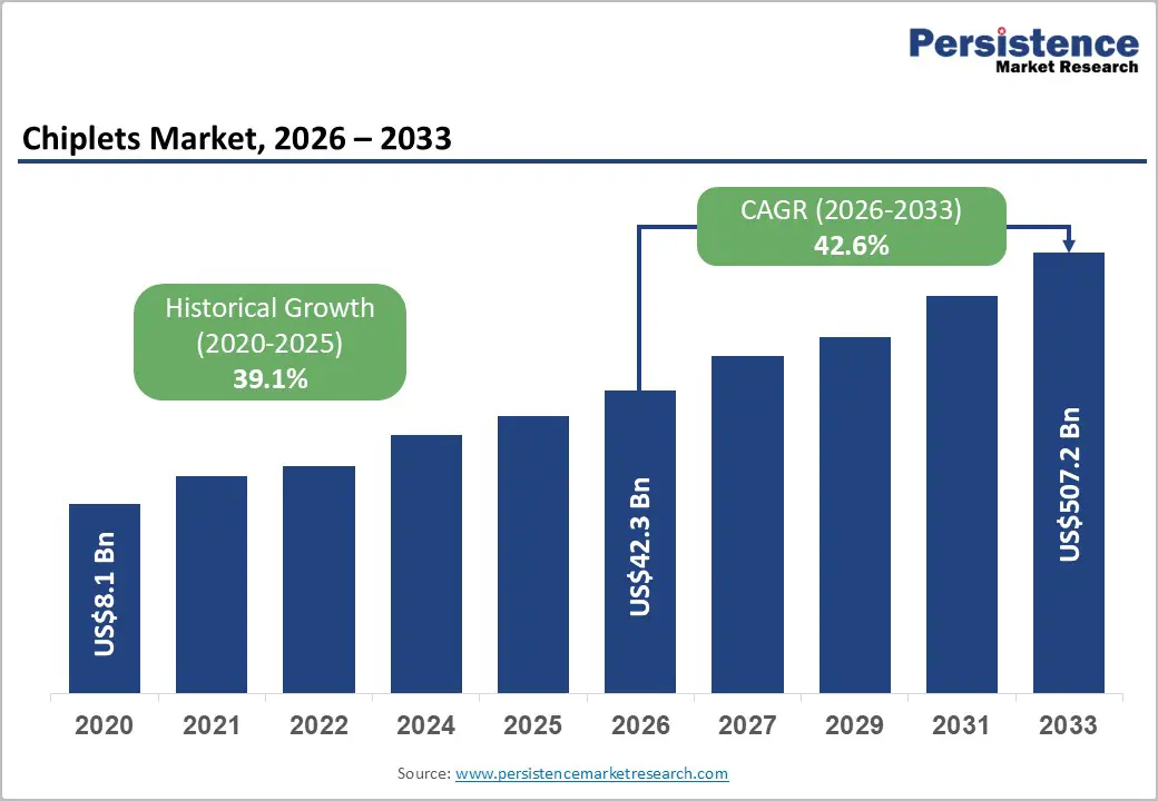
The global chiplets market is entering a transformative phase as artificial intelligence (AI), hyperscale computing, and advanced semiconductor packaging technologies reshape the future of computing architectures. The market is projected to rise from US$ 42.3 billion in 2026 to an impressive US$ 507.2 billion by 2033, registering a remarkable CAGR of 42.6% during the forecast period.
Chiplets are rapidly emerging as a foundational technology for next-generation processors, AI accelerators, high-performance computing (HPC), automotive electronics, and edge AI systems. Unlike traditional monolithic chips, chiplet-based architectures divide functions such as compute, memory, and input/output into smaller modular dies that are integrated within a single package. This modular approach allows semiconductor manufacturers to improve yields, reduce production costs, increase scalability, and accelerate innovation cycles.
The rising complexity of AI workloads, increasing demand for energy-efficient computing, and limitations associated with advanced node scaling are significantly accelerating the transition toward chiplet-enabled semiconductor designs.
AI Revolution Driving Massive Demand for Chiplet Architectures
One of the most significant growth drivers for the chiplets market is the unprecedented expansion of AI infrastructure worldwide. Generative AI, large language models, machine learning, and advanced analytics applications require enormous computational power and memory bandwidth. Traditional monolithic semiconductor designs are increasingly struggling to meet these performance and efficiency requirements.
Chiplets offer an effective solution by enabling the integration of multiple specialized dies within a single package. Compute dies, memory modules, accelerators, and connectivity interfaces can all be optimized independently and then combined using advanced packaging technologies.
Major semiconductor companies are aggressively adopting chiplet strategies for AI-focused platforms. AI accelerators used in training and inference systems require ultra-high bandwidth communication between processors and memory components. Advanced packaging platforms such as CoWoS, Foveros, and EMIB are becoming critical technologies for integrating these chiplet-based systems.
The rapid expansion of hyperscale data centers is also supporting market growth. Cloud providers are investing heavily in AI infrastructure to support growing enterprise demand for generative AI applications, automation, and real-time analytics. This is increasing demand for modular semiconductor architectures that can scale efficiently across massive computing clusters.
Data center and AI accelerator applications are expected to account for nearly 58.7% of the market share in 2026, making them the dominant application segment throughout the forecast period.
Why Chiplets Are Replacing Monolithic Chip Designs
The semiconductor industry is reaching physical and economic limitations with traditional monolithic scaling approaches. As transistor sizes shrink, manufacturing complexity and defect risks increase significantly. Larger monolithic dies are also more expensive to produce and more difficult to yield efficiently.
Chiplets solve many of these challenges through modular design principles. Instead of building one massive chip, manufacturers can design smaller functional dies separately and integrate them into a single package.
This approach provides several advantages:
- Improved manufacturing yields
- Reduced wafer wastage
- Lower development costs
- Faster product iteration cycles
- Enhanced scalability
- Better thermal management
- Flexible heterogeneous integration
Semiconductor companies can now combine chiplets built on different process nodes and even from different vendors. For example, a processor die manufactured using a leading-edge node can be paired with analog or I/O chiplets fabricated using more mature and cost-effective technologies.
This flexibility is becoming essential as semiconductor manufacturers attempt to balance performance, cost efficiency, and supply chain resilience.
Open Interconnect Standards Accelerating Ecosystem Expansion
The rise of open interconnect standards is further strengthening chiplet adoption worldwide. Previously, one of the biggest obstacles to chiplet deployment was the use of proprietary integration frameworks that limited interoperability between vendors.
The introduction of Universal Chiplet Interconnect Express (UCIe) is changing the landscape significantly. Open standards enable interoperability between chiplets manufactured by different companies and fabricated on different process technologies.
The release of UCIe 3.0 in 2025 introduced major improvements in bandwidth, scalability, and multi-chip integration capabilities. These advancements are enabling semiconductor firms, foundries, IP providers, and OEMs to collaborate more efficiently within standardized ecosystems.
Open chiplet ecosystems are expected to create entirely new opportunities for semiconductor innovation. Companies will increasingly specialize in developing optimized chiplets for compute, memory, AI acceleration, networking, or security applications that can be integrated into broader modular systems.
This transition resembles the evolution of software ecosystems, where interoperability accelerated innovation and reduced development barriers across industries.
Asia Pacific Emerging as the Global Chiplet Powerhouse
Asia Pacific is projected to account for approximately 31.2% of the global chiplets market share in 2026 and is also expected to witness the fastest growth through 2033.
The region dominates global semiconductor manufacturing, outsourced semiconductor assembly and test (OSAT) operations, advanced packaging, and foundry services. Countries such as Taiwan, South Korea, China, Japan, and emerging ASEAN economies are investing heavily in semiconductor localization and AI infrastructure.
Taiwan Leading Advanced Packaging Innovation
Taiwan remains central to the global chiplet ecosystem due to its dominance in semiconductor foundry operations and advanced packaging technologies. The country plays a critical role in manufacturing AI accelerators and heterogeneous integration systems used across hyperscale data centers.
Demand for advanced packaging platforms, especially CoWoS, continues to surge as AI chip production expands globally. Packaging capacity expansion in Taiwan is expected to remain one of the key factors supporting long-term market growth.
China Accelerating Semiconductor Self-Sufficiency
China is rapidly expanding investments in semiconductor manufacturing, AI infrastructure, and domestic chip development. Government initiatives aimed at strengthening semiconductor independence are creating strong demand for advanced packaging and chiplet-enabled architectures.
The country’s growing AI server deployment and cloud computing investments are also supporting adoption across enterprise and industrial applications.
India and Southeast Asia Becoming Emerging Packaging Hubs
India and Southeast Asian countries are increasingly investing in semiconductor manufacturing and packaging infrastructure. Government-backed initiatives aimed at building domestic semiconductor ecosystems are expected to create long-term opportunities for chiplet packaging, assembly, and testing operations.
As global companies seek supply chain diversification beyond traditional manufacturing hubs, emerging regional markets are expected to play a larger role in future semiconductor production networks.
Processor Chiplets Dominate Current Market Landscape
Processor chiplets are anticipated to account for approximately 43.5% of market share in 2026, making them the leading component segment.
CPU and GPU compute dies remain the most valuable components within advanced package architectures because they deliver the primary computational capabilities required for AI accelerators, HPC systems, and enterprise servers.
Leading semiconductor companies are increasingly adopting multi-die processor designs to improve scalability and manufacturing efficiency. Chiplet-enabled processors are becoming standard across AI training systems, enterprise computing platforms, and cloud infrastructure.
The success of chiplet-based processors has also encouraged broader industry adoption across networking, telecom, and embedded systems.
Memory Chiplets Becoming Critical for AI Workloads
Memory chiplets are expected to witness the fastest growth during the forecast period due to rising demand for high-bandwidth memory (HBM) integration.
Modern AI models require enormous memory bandwidth and low-latency communication between compute and memory components. HBM stacks integrated alongside GPU and accelerator chiplets are becoming essential for AI servers and large language model training systems.
As AI model complexity continues to rise, demand for advanced memory architectures is expected to grow substantially. Semiconductor memory companies are aggressively expanding production capacity for next-generation HBM technologies to support this demand surge.
The integration of memory chiplets within advanced package architectures is likely to become one of the most critical enablers of future AI infrastructure performance.
Automotive and Edge AI Opening New Growth Opportunities
While data centers currently dominate chiplet adoption, automotive electronics and edge AI are emerging as major future growth areas.
Automotive manufacturers are increasingly integrating chiplet architectures into advanced driver-assistance systems (ADAS), autonomous driving platforms, and software-defined vehicles. Chiplets provide scalability, modularity, and power efficiency that are particularly valuable for automotive applications.
Edge AI systems are also creating strong demand for compact and energy-efficient semiconductor solutions. Industrial automation, robotics, smart cameras, telecom edge servers, and intelligent IoT devices all require high-performance inference processing with low latency and reduced power consumption.
Chiplets allow manufacturers to customize edge computing platforms while maintaining design flexibility and improving lifecycle management.
As 5G infrastructure expands globally, edge AI deployments are expected to accelerate further, strengthening long-term market opportunities.
Packaging Complexity Remains a Major Challenge
Despite the enormous growth potential, the chiplets market still faces several technical and economic challenges.
Advanced packaging technologies such as silicon interposers, fine-pitch bonding, and heterogeneous integration require substantial capital investments and engineering expertise. These packaging methods are significantly more expensive than conventional semiconductor packaging approaches.
System-level validation is also becoming increasingly complex because multiple dies must operate reliably within unified architectures. Engineers must address thermal management, signal integrity, power delivery, and die-to-die communication reliability issues, especially for AI and HPC workloads.
These challenges increase development timelines and raise manufacturing costs, particularly for lower-margin applications.
Currently, chiplet deployment remains concentrated in high-value computing applications where customers can justify premium pricing. Wider adoption across consumer electronics and mass-market devices will depend on future reductions in packaging costs and improvements in manufacturing scalability.
Government Semiconductor Initiatives Creating Long-Term Opportunities
Governments worldwide are investing heavily in semiconductor manufacturing and advanced packaging infrastructure to strengthen supply chain resilience and reduce dependency on foreign suppliers.
The United States, Europe, China, Japan, South Korea, and India are all introducing semiconductor funding programs focused on domestic fabrication, packaging, AI chip development, and research collaboration.
These initiatives are creating opportunities across the semiconductor value chain, including:
- Advanced packaging equipment
- Semiconductor substrates
- Thermal management systems
- Interconnect technologies
- Electronic design automation (EDA)
- Chiplet IP development
- OSAT services
Companies capable of supporting localized semiconductor ecosystems are expected to benefit from strong long-term investment flows and strategic partnerships.
Competitive Landscape Intensifying Across the Semiconductor Ecosystem
The global chiplets market remains moderately fragmented at the semiconductor design level, although advanced packaging capacity remains concentrated among a relatively small number of global providers.
Leading companies are competing aggressively through:
- Advanced packaging innovation
- AI-focused semiconductor development
- Open interconnect ecosystem participation
- Strategic foundry partnerships
- Regional capacity expansion
- Heterogeneous integration capabilities
Major industry participants include Taiwan Semiconductor Manufacturing Company, NVIDIA Corporation, Advanced Micro Devices, Intel Corporation, Samsung Electronics, ASE Technology Holding, Amkor Technology, Broadcom, Qualcomm, Marvell Technology, Micron Technology, SK hynix, Synopsys, Cadence Design Systems, Arm Holdings, and IBM Corporation.
Strategic collaborations between semiconductor firms, hyperscalers, foundries, and packaging providers are expected to intensify as AI computing requirements continue to grow.
Future Outlook
The chiplets market is poised to become one of the fastest-growing segments within the global semiconductor industry. AI infrastructure expansion, advanced packaging innovation, heterogeneous integration, and semiconductor localization initiatives are collectively reshaping the future of chip design.
As performance requirements increase and traditional scaling approaches become less sustainable, chiplets are expected to evolve from a premium computing solution into a mainstream semiconductor architecture.
Future advancements in packaging efficiency, interconnect standards, and manufacturing scalability will determine how rapidly chiplets expand across automotive electronics, edge AI, industrial automation, telecommunications, and consumer computing applications.
With AI transforming nearly every industry, chiplet-enabled architectures are expected to play a foundational role in powering the next generation of intelligent computing systems worldwide.

 Arabic
 French
 Spanish
 Portuguese
 Deutsch
 Turkish
 Dutch
Dutch
 Italiano
 Russian
 Romaian
 Portuguese (Brazil)
 Greek
Greek