


Nanopatterning Market Overview
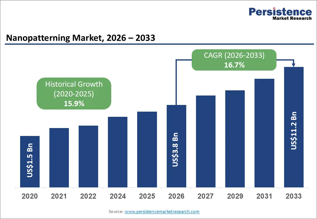
The global nanopatterning market is entering a high-growth phase as industries accelerate the transition toward smaller, faster, and more efficient electronic and photonic devices. The market size is projected to reach US$3.8 billion in 2026 and is expected to expand to US$11.2 billion by 2033, registering a strong CAGR of 16.7% between 2026 and 2033.
The rapid expansion of the market is primarily fueled by the growing demand for semiconductor miniaturization, advanced chip architectures, next-generation lithography technologies, and increasing adoption of nanotechnology across healthcare, photonics, consumer electronics, and quantum computing applications.
Nanopatterning refers to a collection of advanced fabrication techniques used to create nanoscale structures and patterns, typically below 100 nanometers, with extreme precision. These technologies enable the production of advanced semiconductor devices, nanophotonic components, biosensors, flexible electronics, quantum devices, and highly engineered nanostructured surfaces that cannot be achieved through conventional manufacturing processes.
As semiconductor manufacturers move toward sub-5nm and 2nm process nodes while expanding advanced packaging and heterogeneous integration, nanopatterning technologies are becoming increasingly critical for maintaining performance improvements and enabling future generations of electronic systems.
Semiconductor Miniaturization: The Core Growth Engine for Nanopatterning
The most significant factor driving nanopatterning market growth is the continuous demand for semiconductor scaling and enhanced chip performance. The semiconductor industry is experiencing unprecedented pressure to manufacture smaller transistors with higher efficiency, lower power consumption, and improved processing capabilities.
Advanced manufacturing nodes from leading semiconductor companies such as TSMC, Samsung Electronics, and Intel require extremely precise nanoscale patterning technologies.
TSMC’s advanced 3nm and upcoming 2nm manufacturing processes, Samsung’s Gate-All-Around (GAA) transistor architecture, and Intel’s advanced process technologies depend heavily on extreme precision lithography and nanoscale fabrication methods.
Extreme ultraviolet (EUV) lithography has become a major contributor to this transformation, creating demand for:
- EUV-compatible photoresists
- Advanced photomasks
- Mask blanks
- High-resolution patterning systems
- Defect-control technologies
The continued expansion of artificial intelligence chips, high-performance computing, 5G infrastructure, automotive semiconductors, and data center processors is expected to further accelerate demand for nanopatterning solutions.
Key Market Highlights
Asia Pacific Dominates the Global Nanopatterning Market
Asia Pacific is expected to maintain its leadership position, accounting for approximately 38% of global nanopatterning market revenue in 2026.
The region’s dominance is supported by:
- Large-scale semiconductor manufacturing facilities
- Strong presence of foundries and integrated device manufacturers
- Government-backed nanotechnology initiatives
- Increasing investments in advanced semiconductor fabrication
Countries including Taiwan, South Korea, Japan, China, and India are becoming major centers for nanoscale manufacturing innovation.
Taiwan continues to lead through its semiconductor ecosystem, particularly through TSMC’s advanced fabrication facilities. South Korea remains a key contributor due to Samsung’s investments in advanced memory and logic semiconductor technologies.
Japan continues to strengthen its position through advanced materials, lithography research, and nanofabrication expertise, while China is rapidly expanding domestic semiconductor and nanotechnology capabilities.
India is also emerging as a growing semiconductor and nanotechnology hub through initiatives supporting domestic manufacturing, semiconductor packaging, and research infrastructure.
E-Beam Lithography Leads the Nanopatterning Technology Market
Among different nanopatterning technologies, electron-beam lithography (E-beam lithography) is expected to dominate the market, capturing approximately 34% revenue share in 2026.
The technology remains highly preferred because of its unmatched resolution capabilities and ability to create extremely small patterns without requiring physical masks.
E-beam lithography enables:
- Sub-10nm pattern creation
- Photomask manufacturing
- Prototype semiconductor development
- Quantum device fabrication
- Research-scale nanostructure production
Companies such as Vistec Electron Beam GmbH, JEOL Ltd., and IMS Nanofabrication GmbH are actively developing advanced e-beam systems to meet rising demand from semiconductor manufacturers and research institutions.
JEOL’s JBX electron beam lithography systems are widely used for semiconductor research, photomask production, and advanced nanodevice development.
However, despite its exceptional resolution, e-beam lithography faces limitations in production environments because of relatively slow writing speeds compared with high-volume manufacturing technologies.
Nanoimprint Lithography Emerges as the Fastest-Growing Segment
Nanoimprint lithography (NIL) is expected to experience the fastest growth among nanopatterning technologies due to its advantages in throughput, cost efficiency, and scalability.
Unlike traditional lithography techniques, NIL uses a physical mold or template to transfer nanoscale patterns onto surfaces, making it highly suitable for applications requiring large-scale production.
Growing adoption areas include:
- Organic electronics
- Micro-LED displays
- Optical components
- Biosensors
- Magnetic storage devices
- Advanced packaging
Canon’s nanoimprint lithography platforms, including the FPA-1200NZ2C, represent significant progress toward commercializing NIL technology for semiconductor manufacturing.
The ability of NIL to reduce manufacturing costs while achieving high-resolution patterns makes it an attractive alternative for specific semiconductor and electronics applications.
Consumer Electronics Remains the Largest Application Segment
The consumer electronics sector is expected to represent approximately 42% of nanopatterning market revenue in 2026, making it the largest application category.
Modern electronic devices increasingly depend on nanoscale manufacturing technologies to deliver:
- Higher processing power
- Smaller device footprints
- Improved battery efficiency
- Advanced display performance
- Enhanced connectivity
Nanopatterning plays a critical role in manufacturing:
- Smartphone processors
- OLED and MicroLED displays
- Camera sensors
- 5G communication components
- Wearable electronics
Companies such as Samsung Electronics use advanced nanoscale fabrication techniques for next-generation OLED, QD-OLED, and MicroLED display technologies.
Healthcare Creates New Growth Opportunities
Healthcare is expected to become the fastest-growing application area for nanopatterning technology.
The combination of nanotechnology and biomedical innovation is opening new opportunities in:
- Point-of-care diagnostics
- Biosensors
- Lab-on-chip devices
- Drug delivery systems
- Medical implants
Nanopatterned surfaces improve biological interactions and enable highly sensitive detection systems.
For example, silicon photonic biosensors developed through nanopatterning techniques can detect biomarkers associated with diseases such as cancer at early stages.
The increasing demand for personalized medicine and rapid diagnostics is expected to create significant opportunities for nanopatterning equipment manufacturers.
Quantum Computing and Photonics: Emerging High-Value Opportunities
Quantum technologies represent one of the most promising future applications for nanopatterning.
Quantum computing devices require extremely precise nanoscale structures for manufacturing:
- Superconducting qubit components
- Quantum dots
- Single-photon detectors
- Photonic crystal structures
Similarly, advanced photonics applications are driving demand for nanopatterning in:
- Silicon photonics
- Optical communication systems
- LiDAR sensors
- Data center connectivity
- Environmental sensing platforms
As artificial intelligence workloads increase global data traffic, photonic technologies requiring nanoscale fabrication are expected to experience rapid adoption.
Market Challenges: Complexity and Cost Constraints
Despite strong growth prospects, nanopatterning technologies face several challenges.
High Manufacturing Complexity
Advanced nanopatterning requires extremely precise equipment and controlled environments. Maintaining nanoscale accuracy while minimizing defects remains a major technical challenge.
Nanoimprint Lithography Template Costs
Although NIL provides cost advantages during high-volume production, template manufacturing remains expensive.
Nanoimprint templates require:
- Sub-nanometer precision
- Advanced fabrication techniques
- High-quality defect control
Additionally, repeated usage can cause template degradation, leading to replacement costs and affecting overall manufacturing economics.
Regional Market Analysis
North America
North America remains a major innovation center for nanopatterning due to strong semiconductor research, advanced packaging development, and quantum technology investments.
The United States leads the regional market with contributions from:
- Intel
- IBM
- National laboratories
- University nanofabrication facilities
Demand is supported by investments in advanced semiconductor manufacturing, AI processors, and quantum computing technologies.
Canada is also emerging as a growing contributor through research programs focused on nanomaterials, photonics, and biomedical applications.
Europe
Europe represents a significant nanopatterning market supported by strong research infrastructure and semiconductor expertise.
Germany is a leading regional contributor due to:
- Semiconductor manufacturing capabilities
- Automotive electronics demand
- Photonics expertise
- MEMS innovation
The United Kingdom also plays an important role through university-led nanotechnology research and quantum technology development.
Asia Pacific
Asia Pacific is expected to remain the fastest-growing regional market through 2033.
Growth is driven by:
- Semiconductor manufacturing expansion
- Advanced packaging adoption
- Consumer electronics production
- Government investments in nanotechnology
China, Japan, South Korea, Taiwan, and India are expected to remain central contributors to market expansion.
Competitive Landscape
The nanopatterning market is characterized by specialized technology providers focusing on different fabrication approaches.
Major companies operating in the market include:
- EV Group
- Vistec Electron Beam GmbH
- Nanoscribe GmbH & Co. KG
- Nanonex Corp.
- NIL Technology ApS
- Micro Resist Technology GmbH
- Fraunhofer Gesellschaft
- Meta Materials Inc.
- Nippon Telegraph and Telephone Corporation
- Institute for Microelectronics Stuttgart
Companies compete based on:
- Pattern resolution
- Throughput
- Equipment reliability
- Material compatibility
- Application-specific performance
Technology specialization remains a key competitive advantage, with companies focusing on specific niches such as e-beam lithography, nanoimprint systems, photonics fabrication, and biomedical nanostructuring.
Recent Industry Developments
In 2024, ASML Holding NV and Tokyo Electron Limited announced collaboration efforts focused on advancing EUV lithography technologies for semiconductor manufacturing. The initiative aims to accelerate next-generation chip production using advanced nanopatterning techniques.
Intel also introduced advanced semiconductor technologies incorporating nanoscale manufacturing approaches to improve transistor density and performance for future process generations.
Future Outlook for the Nanopatterning Market
The nanopatterning market is positioned for significant expansion as industries continue pushing the boundaries of miniaturization and precision manufacturing.
Between 2026 and 2033, market growth will be shaped by:
- Expansion of advanced semiconductor nodes
- Increasing AI and high-performance computing demand
- Growth of quantum technologies
- Rising adoption of nanophotonic systems
- Healthcare innovation through nanoscale devices
- Development of next-generation electronics
With semiconductor manufacturers requiring increasingly sophisticated fabrication capabilities, nanopatterning will remain a foundational technology enabling the future of computing, communication, healthcare, and advanced manufacturing.
The market’s projected growth from US$3.8 billion in 2026 to US$11.2 billion by 2033 highlights the strategic importance of nanoscale fabrication technologies in shaping the next era of technological innovation.

 English
 Arabic
 French
 Spanish
 Portuguese
 Deutsch
 Turkish
 Dutch
Dutch
 Russian
 Romaian
 Portuguese (Brazil)
 Greek
Greek