


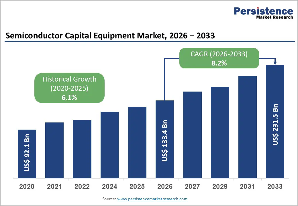
The global semiconductor capital equipment market is entering a phase of sustained structural expansion, driven by unprecedented demand for advanced chips across artificial intelligence (AI), high-performance computing (HPC), automotive electronics, and next-generation communication infrastructure. The market size is projected to grow from US$133.4 billion in 2026 to US$231.5 billion by 2033, registering a CAGR of 8.2% during the forecast period.
This strong growth trajectory reflects a fundamental shift in global semiconductor strategy, where governments and private enterprises are aggressively investing in fabrication capacity, advanced process nodes, and supply chain resilience. Technologies such as Extreme Ultraviolet (EUV) lithography and High-NA EUV are redefining manufacturing complexity, increasing reliance on high-value capital equipment.
The market is also being reshaped by geopolitical realignment, semiconductor sovereignty initiatives, and rapid technological transitions toward chiplet-based architectures and heterogeneous integration.
Market Overview and Growth Drivers
AI, Cloud Computing, and Advanced Node Expansion
One of the most powerful growth drivers is the explosive rise of AI workloads and hyperscale data centers. Training large language models and deploying AI inference at scale require cutting-edge chips manufactured at 5 nm, 3 nm, and emerging 2 nm nodes. These advanced nodes depend on highly sophisticated wafer fabrication equipment, including lithography, deposition, etching, and metrology systems.
Leading semiconductor manufacturers such as Taiwan Semiconductor Manufacturing Company (TSMC), Intel Corporation, and Samsung Electronics are significantly increasing capital expenditure to support AI-driven chip demand. As process geometries shrink, equipment intensity per wafer rises sharply, boosting long-term demand for capital equipment.
Government-Led Semiconductor Expansion
Government initiatives are another key catalyst. Programs such as the U.S. CHIPS and Science Act and the European Chips Act are incentivizing domestic semiconductor manufacturing. These policies are driving new fabrication plant (fab) construction across North America and Europe.
Countries including China, Japan, India, Germany, and South Korea are also investing heavily in semiconductor sovereignty programs. This global expansion is creating sustained demand for wafer fabrication equipment (WFE), advanced packaging systems, and testing solutions.
Market Restraints
Cyclical Demand and Inventory Corrections
Despite strong long-term growth, the semiconductor capital equipment market remains highly cyclical. Demand is closely tied to semiconductor end markets such as smartphones, PCs, and memory chips. When demand weakens, semiconductor manufacturers reduce capital spending, leading to order cancellations or delays.
The downturn in NAND and DRAM markets in recent cycles highlighted this vulnerability, as oversupply and lower utilization rates forced manufacturers to scale back investments. This cyclicality creates volatility for equipment vendors and impacts revenue predictability.
Geopolitical Restrictions and Export Controls
Geopolitical tensions continue to shape the competitive landscape. Export restrictions on advanced semiconductor tools—particularly EUV and advanced DUV lithography systems—have restricted access for certain regions.
Companies like ASML Holding, a critical supplier of EUV lithography systems, face complex compliance requirements when shipping advanced tools. These restrictions have fragmented global supply chains and limited the addressable market in certain geographies, particularly China.
Market Opportunities
Advanced Packaging and Chiplet Architectures
One of the most significant opportunities lies in advanced packaging technologies such as 2.5D and 3D integration, wafer-level packaging, and chiplet architectures. As traditional Moore’s Law scaling slows, manufacturers are increasingly relying on advanced packaging to improve performance and efficiency.
These architectures require new equipment categories, including high-precision bonding tools, inspection systems, and wafer-level testing platforms. Companies such as Applied Materials and Lam Research Corporation are expanding their portfolios to address this high-growth segment.
Power Semiconductors and EV Revolution
The rise of electric vehicles (EVs), renewable energy systems, and industrial electrification is boosting demand for power semiconductors such as SiC (silicon carbide) and GaN (gallium nitride) devices.
These applications require specialized fabrication tools capable of handling high voltages and wide-bandgap materials. As automotive electrification accelerates, new fabs dedicated to power devices are expected to significantly increase capital equipment demand.
Market Segmentation Analysis
By Equipment Type
Wafer Fabrication Equipment (WFE) dominates the market, accounting for over 84% share in 2026, valued at more than US$112 billion. This segment includes lithography, etching, deposition, ion implantation, and cleaning systems, all essential for advanced chip manufacturing.
As nodes shrink below 3 nm, WFE demand intensifies due to rising process complexity and precision requirements.
Meanwhile, assembly and packaging equipment is the fastest-growing segment, driven by chiplet integration, heterogeneous computing, and advanced 3D packaging technologies.
By Application
The foundry/logic segment leads with over 46% market share in 2026, valued at more than US$61.4 billion. The growth is driven by rising demand for AI processors, GPUs, and advanced SoCs used in data centers and mobile devices.
The fastest-growing segment is discrete and power devices, supported by EV adoption, renewable energy expansion, and industrial automation.
By Industry Vertical
The consumer electronics sector dominates with over 34% share in 2026, driven by smartphones, laptops, wearables, and smart home devices.
However, the automotive sector is the fastest-growing, expanding at a CAGR of 11.9% due to increasing semiconductor content per vehicle. Modern vehicles now rely heavily on chips for ADAS, infotainment, battery management systems, and autonomous driving capabilities.
Regional Analysis
Asia Pacific
Asia Pacific leads the global market with over 62% share in 2026, valued at approximately US$82.7 billion. The region benefits from strong semiconductor ecosystems in Taiwan, South Korea, Japan, and China, supported by major foundries and memory manufacturers.
This region remains the global hub for wafer fabrication and continues to attract large-scale investments in advanced nodes and memory production.
North America
North America is experiencing strong growth due to government-backed initiatives such as the CHIPS Act. New fab investments by companies including Intel Corporation and Samsung Electronics in the United States are driving demand for advanced manufacturing equipment.
The presence of major equipment manufacturers like Applied Materials, Lam Research Corporation, and KLA Corporation further strengthens the region’s leadership in innovation.
Europe
Europe plays a strategic role in semiconductor capital equipment due to its leadership in lithography technology. ASML Holding, based in the Netherlands, is the world’s only supplier of EUV lithography systems, making it indispensable for sub-5 nm manufacturing.
The European Chips Act aims to significantly expand regional semiconductor production, particularly for automotive and industrial applications.
Competitive Landscape
The semiconductor capital equipment market is highly concentrated, dominated by a small group of global leaders with strong technological differentiation and high entry barriers.
Key companies include:
- ASML Holding – Leader in EUV lithography systems
- Applied Materials – Dominant in deposition and materials engineering
- Lam Research Corporation – Leader in etch and deposition technologies
- KLA Corporation – Advanced process control and inspection systems
- Tokyo Electron Limited – Major player in wafer processing equipment
- Teradyne Inc. – Semiconductor testing solutions
These companies are investing heavily in R&D, automation, AI-based process optimization, and predictive maintenance systems to enhance fab efficiency.
Recent Developments
Recent industry developments highlight continued innovation:
- Lam Research Corporation expanded its R&D footprint in Idaho to support advanced memory and AI chip production, strengthening collaboration with memory manufacturers.
- Nikon Corporation introduced advanced digital lithography systems designed for next-generation semiconductor packaging, improving precision and productivity in advanced manufacturing.
Conclusion
The semiconductor capital equipment market is undergoing a transformative growth phase driven by AI, advanced computing, automotive electrification, and global semiconductor localization strategies. With market value expected to nearly double by 2033, equipment demand will remain structurally strong across wafer fabrication, packaging, and testing segments.
However, the industry will continue to navigate cyclical volatility and geopolitical complexity. In this environment, companies with strong technological leadership, diversified portfolios, and deep partnerships with leading fabs will be best positioned to capture long-term growth opportunities.
Overall, semiconductor capital equipment remains a foundational pillar of the global digital economy, enabling the next generation of computing, connectivity, and intelligent systems.

 English
 Arabic
 French
 Spanish
 Portuguese
 Deutsch
 Turkish
 Italiano
 Russian
 Romaian
 Portuguese (Brazil)
 Greek
Greek