


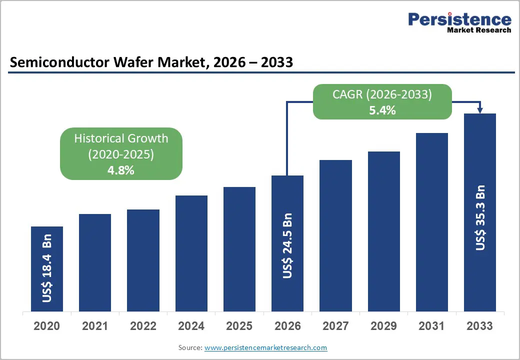
The global semiconductor wafer market is entering a structurally transformative growth phase, driven by the convergence of advanced computing, automotive electrification, and strategic national investments in semiconductor self-sufficiency. Valued at US$ 24.5 billion in 2026, the market is projected to reach US$ 35.3 billion by 2033, expanding at a CAGR of 5.4% during the forecast period.
From its historical level of US$ 18.4 billion in 2020, the industry has steadily expanded, supported by rising chip complexity, surging digital demand, and the rapid scaling of wafer fabrication capacities across key global hubs.
At its core, the semiconductor wafer market forms the foundation of the entire semiconductor ecosystem. Every processor, memory chip, sensor, and power device begins its lifecycle on a wafer substrate—making this market a critical upstream enabler of global digital infrastructure.
Market Overview and Growth Drivers
The semiconductor wafer market is being shaped by four powerful structural forces:
First, the rise of artificial intelligence (AI) and advanced-node computing is accelerating demand for ultra-high-purity, large-diameter wafers. AI chips require extremely complex architectures built on leading-edge nodes below 5nm, which depend heavily on 300 mm wafer substrates for cost efficiency and yield optimization.
Second, the electrification of vehicles and industrial systems is significantly boosting demand for compound semiconductor wafers such as silicon carbide (SiC) and gallium nitride (GaN). These materials are essential for high-efficiency power electronics used in electric vehicles (EVs), fast-charging infrastructure, and renewable energy systems.
Third, governments across major economies are actively pursuing semiconductor reindustrialization strategies. Policies such as the U.S. CHIPS and Science Act, the European Chips Act, and India’s Semicon India Programme are collectively reshaping global wafer supply chains.
Fourth, the industry is witnessing a migration toward larger wafer diameters, particularly 300 mm substrates, which offer superior economies of scale and improved manufacturing efficiency.
Key Industry Highlights
Asia Pacific remains the dominant region, accounting for 66.5% of global market share, supported by strong semiconductor ecosystems in Taiwan, South Korea, Japan, and China. India is emerging as a new growth frontier, backed by government incentives and rising domestic demand.
North America holds approximately 16.0% share, driven by policy-led investments under the CHIPS Act and expanding domestic wafer production capacity, including new 300 mm fabrication facilities.
The 300 mm wafer segment dominates with 68.5% share, serving as the backbone for advanced logic and memory devices used in AI and high-performance computing applications.
The 200 mm wafer segment is the fastest-growing, particularly due to demand from power semiconductor applications such as EVs and industrial electronics.
In terms of materials, silicon wafers account for nearly 89% of the market, while compound semiconductor wafers are expanding at the fastest rate, driven by EVs, 5G, and next-generation power systems.
Logic devices remain the largest consumption category, representing 34% of wafer demand, fueled by rapid AI chip expansion.
DRO Analysis
Government-Led Semiconductor Reindustrialization
Government intervention has become one of the most influential forces shaping the semiconductor wafer market. Countries are no longer treating semiconductor production as a purely commercial activity but as a strategic national capability.
The United States has allocated US$ 52.7 billion under the CHIPS and Science Act, including incentives for fabrication expansion and R&D investment. This has triggered a wave of domestic wafer manufacturing projects, including large-scale 300 mm facilities.
Europe’s Chips Act has mobilized over €43 billion in public and private funding, targeting the strengthening of regional semiconductor ecosystems and reducing dependency on external suppliers.
India’s Semicon India Programme, with commitments of INR 76,000 crore, is actively developing domestic wafer capabilities through approved silicon and SiC fabrication projects. These initiatives are establishing new demand corridors for wafer manufacturers globally.
Generative AI and Advanced-Node Demand
The emergence of generative AI has fundamentally redefined wafer demand dynamics. AI workloads require extremely high-performance chips built on advanced logic nodes, which in turn depend on cutting-edge wafer substrates.
Global logic semiconductor sales reached US$ 212.6 billion in 2024, making it the largest semiconductor segment. Memory chips also surged sharply, with DRAM demand experiencing strong cyclical growth.
Leading wafer manufacturers are responding accordingly. Companies such as SUMCO are prioritizing upgrades for next-generation wafers beyond the 2nm node, while GlobalWafers is expanding 300 mm capacity in the United States to support AI-driven chip demand.
Electrification of Automotive Platforms
The automotive industry is undergoing a structural shift toward electrification, creating strong demand for compound semiconductor wafers.
Electric vehicles now account for approximately 38% of total automotive semiconductor usage, with semiconductor content per vehicle increasing by more than 45% compared to traditional vehicles.
SiC and GaN wafers are critical for EV powertrains, onboard chargers, and fast-charging systems. These materials offer higher efficiency, thermal stability, and energy savings compared to traditional silicon.
As EV adoption accelerates globally, demand for wide-bandgap wafers is expected to remain a key structural growth driver.
Market Restraints
Despite strong growth prospects, the semiconductor wafer market faces several structural constraints.
One of the most significant challenges is pricing pressure and inventory cyclicality. Periodic oversupply in mature nodes leads to price erosion, especially in 200 mm wafer segments used in power semiconductors and industrial applications.
Another major restraint is high capital intensity. Wafer manufacturing requires billions of dollars in investment, making capacity expansion slow and financially demanding. Advanced fabs require highly specialized infrastructure, cleanrooms, and precision equipment.
Additionally, the industry is highly concentrated geographically in Taiwan, Japan, and South Korea. This concentration creates supply chain vulnerability, exposing downstream industries to geopolitical and logistical risks.
Market Opportunities
Despite challenges, the semiconductor wafer market presents substantial long-term opportunities.
A major opportunity lies in the localization of wafer manufacturing in emerging economies. India, Southeast Asia, and parts of Europe are actively building domestic semiconductor ecosystems supported by government incentives.
India’s entry into wafer fabrication, including silicon and SiC projects, represents a significant shift toward geographic diversification of the global supply chain.
Another major opportunity is the rapid expansion of compound semiconductor applications. SiC and GaN wafers are increasingly used in EVs, AI data centers, and 5G infrastructure, creating a multi-industry demand base.
Advancements in 300 mm SiC and GaN wafer production are also expected to reduce costs and accelerate adoption across high-growth sectors.
Category-Wise Analysis
Wafer Size
The 300 mm wafer segment dominates global demand, accounting for nearly 68.5% of the market. These wafers are essential for advanced-node logic and memory chips, particularly in AI and high-performance computing applications.
Manufacturers are increasingly shifting away from smaller wafer sizes, as seen in industry decisions to phase out certain 150 mm and 200 mm capacities.
Meanwhile, the 200 mm segment remains strategically important, especially for power semiconductors and analog applications. Its growth is supported by EV adoption and industrial electrification.
Material Type
Silicon remains the dominant material, representing nearly 89% of total wafer consumption. It continues to serve as the backbone of the global semiconductor ecosystem due to its cost efficiency and scalability.
However, compound semiconductor wafers are growing rapidly, driven by applications requiring high efficiency and high power density. SiC and GaN materials are particularly important for EVs and renewable energy systems.
Device Type
Logic devices dominate wafer consumption, accounting for approximately 34% of total demand. This reflects the increasing importance of AI, cloud computing, and high-performance processors.
Memory devices represent the fastest-evolving segment, supported by the growing demand for high-bandwidth memory (HBM) in AI accelerators and data center applications.
Regional Insights
Asia Pacific
Asia Pacific leads the global semiconductor wafer market with 66.5% share. Taiwan remains the global hub for advanced semiconductor fabrication, while South Korea and Japan dominate memory and materials supply chains.
China continues to expand its domestic semiconductor capabilities, while India is emerging as a new strategic player supported by government-led investment programs.
North America
North America holds 16% market share, with growth driven by U.S. policy support under the CHIPS Act. The region is witnessing a resurgence in domestic semiconductor manufacturing, including new wafer fabrication facilities and capacity expansions.
Europe
Europe accounts for 12.5% of the market, supported by strong materials expertise and research institutions. While the region remains technologically advanced, it faces challenges in scaling wafer production compared to Asia.
Competitive Landscape
The semiconductor wafer market is highly consolidated, with a small group of major players dominating global supply.
Key companies include Shin-Etsu Chemical, SUMCO Corporation, GlobalWafers, Siltronic AG, and SK Siltron. These firms collectively control the majority of global silicon wafer production.
Competition is increasingly focused on technological advancement, particularly in ultra-pure silicon, 300 mm wafer scaling, and compound semiconductor expansion.
Strategic geographic expansion, especially into the U.S. and India, is a key competitive priority. Long-term supply agreements with leading semiconductor fabs further strengthen market positioning.
Recent Developments
In 2024, Siltronic AG announced the phase-out of small-diameter wafer production, signaling a shift toward advanced-node-focused manufacturing.
GlobalWafers continues to expand its U.S. footprint with a major 300 mm wafer facility in Texas, reinforcing domestic supply chain resilience.
These developments highlight the industry's transition toward large-scale, high-efficiency wafer production aligned with AI and electrification trends.
Conclusion
The semiconductor wafer market is undergoing a profound structural transformation. While historically driven by steady demand from consumer electronics, the industry is now being reshaped by AI computing, automotive electrification, and government-backed industrial policy.
Between 2026 and 2033, growth will increasingly depend on advanced-node innovation, compound semiconductor adoption, and regional supply chain diversification.
As wafers remain the foundational substrate of all semiconductor technologies, their strategic importance will continue to intensify, positioning this market at the center of the global digital economy.

 English
 French
 Spanish
 Portuguese
 Deutsch
 Turkish
 Dutch
Dutch
 Italiano
 Russian
 Romaian
 Portuguese (Brazil)
 Greek
Greek